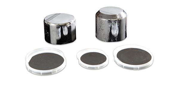
公司投产了具有国际先进水平的2-4英寸磷化铟衬底生产线。产品被广泛应用于微波振荡器与放大器、光纤通讯功率放大器以及激光武器功率放大器等领域。
We set up a produceing line of 2’’ to 4’’ semi-conducting & semi-insulating InP wafer producing. They are wildly used in microwave oscillator & amplifier, amplifier for optical communication & power amplifier for laser weapons.
半导体磷化铟规格 Specifications of semi-conducting InP wafer
|
生长方法 |
VGF |
||
|
掺杂类型 |
P型:锌 |
N型:硫,锡,无掺杂 |
|
|
晶片形状 |
圆形(尺寸2、3、4英寸) |
||
|
晶向 |
(100)±0.5° |
||
|
* Other Orientations maybe available upon request |
|||
|
Dopant |
硫,锡(N型) |
无掺杂(N型) |
锌(P型) |
|
载流子浓度 |
( 0.8-8) × 1018 |
( 1-10) × 1015 |
( 0.8-8) × 1018 |
|
迁移率 |
( 1-2.5) × 103 |
( 3-5) × 103 |
50-100 |
|
位错 |
100-5,000 |
≤ 5000 |
≤ 500 |
|
直径 |
50.8±0.3 |
76.2±0.3 |
100±0.3 |
|
厚度 |
350±25 |
625±25 |
625±25 |
|
TTV [P/P] (µm) |
≤ 10 |
≤ 10 |
≤ 10 |
|
TTV [P/E] (µm) |
≤ 10 |
≤ 15 |
≤ 15 |
|
WARP (µm) |
≤ 15 |
≤ 15 |
≤ 15 |
|
OF (mm) |
17±1 |
22±1 |
32.5±1 |
|
OF / IF (mm) |
7±1 |
12±1 |
18±1 |
|
Polish* |
E/E, |
E/E, |
E/E, |
|
*E=Etched, P=Polished(*E=腐蚀, P=抛光) |
|||
|
**If needed by customer |
|||
半绝缘磷化铟规格 Specifications of semi-insulating InP wafer
|
生长方法 |
VGF |
||
|
掺杂类型 |
SI 型:铁 |
||
|
晶片形状 |
圆形(尺寸2、3、4英寸) |
||
|
晶向 |
(100)±0.5° |
||
|
*OtherOrientationsmaybeavailableuponrequest |
|||
|
电阻率 |
≥ 0.5× 10⁷ |
||
|
迁移率 |
≥ 1,000 |
||
|
位错 |
1,500-5,000 |
||
|
直径 |
50.8±0.3 |
76.2±0.3 |
100±0.3 |
|
厚度 |
350±25 |
625±25 |
625±25 |
|
TTV[P/P](µm) |
≤ 10 |
≤ 10 |
≤ 10 |
|
TTV[P/E](µm) |
≤ 10 |
≤ 15 |
≤ 15 |
|
WARP(µm) |
≤ 15 |
≤ 15 |
≤ 15 |
|
OF (mm) |
17±1 |
22±1 |
32.5±1 |
|
OF / IF (mm) |
7±1 |
12±1 |
18±1 |
|
Polish* |
E/E, |
E/E, |
E/E, |
|
*E=Etched, P=Polished(*E=腐蚀, P=抛光) |
|||
|
**Ifneededbycustomer |
|||
